
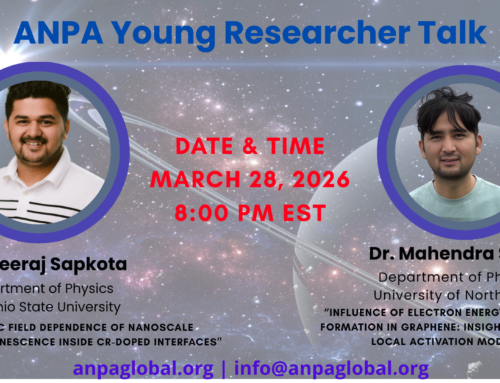
For the colloquium series, this month we feature two Young Researchers’ talks.
The first presenter is Mr. Deeraj Sapkota, a graduate student in the Physics Department at The Ohio State University. The title of his presentation is “Unlocking the Mysteries of the Universe with Neutrinos.”
Chromium (Cr) is a common impurity in crystals, where its characteristic R1 and R2 luminescence lines are susceptible to both the host crystal field and externally applied fields. In this work, we demonstrate that the Cr cathodoluminescence (CL) quenches toward the bulk of the crystal but enhances with applied reverse bias, reflecting the effect of free carrier depletion with increasing electric field. Furthermore, we illustrate that the R1/R2 CL intensity ratio, measured as the integrated area ratio of R1 to R2, can be used as a direct probe of the electric field in a Ni- Schottky diode. This optical calibration method provides a complementary approach to conventional C-V and I-V measurements for determining electric field strength in the depletion region of -based Schottky diodes and can be extended to other semiconductors and multilayer device structures.
Our next presenter is Dr. Mahendra Subedi, who is a recent PhD awardee from the University of North Texas, Department of Physics and Astronomy. The title of his talk is “Influence of electron energy on defect formation in graphene: Insights from the local activation model.”
We investigate the effects of electron beam energy on defect formation in monolayer graphene using Raman spectroscopy and the local activation model. Monolayer graphene samples were irradiated at beam energies ranging from 1 to 30 keV, and the evolution of Raman D, G, and D’ peaks was monitored as a function of electron fluence. For all energies, the ID/IG and ID′/IG ratios exhibited a two-stage behavior, initially increasing with fluence before decreasing at higher defect densities, consistent with the local activation model predictions. Notably, the maximum ID/IG ratio decreased and shifted to a higher fluence with increasing beam energy. At lower beam energies (1–2 keV), an additional broad Raman peak was observed near the G peak, attributed to carbonaceous film deposition from secondary electrons (SEs). Defect formation was modeled using the local activation model with adjustments to account for SE-induced dissociation of surface adsorbates, showing good agreement with experimental data. Parameters A and B, which represent the incident electron fluence required to generate a defect-active region and the fraction of dissociable adsorbates, respectively, showed systematic trends with beam energy. Postirradiation annealing studies were conducted to determine activation energies for defect healing via Arrhenius analysis. The extracted activation energies (0.31–0.48 eV) are consistent with sp3-type defects such as hydrogen and hydroxyl groups with attached water molecules. These findings highlight the critical role of beam energy and SE yield in the defect engineering of graphene and demonstrate the utility of the local activation model in quantitatively describing beam-induced disorder.
Date and Time:
Saturday, March 28th, 2026 at 8:00 PM US ET,
(Nepal Time: Sunday, 5:45 AM Chaitra, 15th, 2082 in Nepal)
Webex link will be provided to ANPA members via email.
For others interested, please use this link to register to get the meeting link.


Leave A Comment